Fabrication and characterization of solid state nanostructures
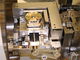
The Walther-Meissner-Institute uses advanced nanofabrication technologies to realize metallic, superconducting and magnetic nanostructures. The nanostructures are achieved by the top-down method by the nano-patterning of thin film structures. We are using a Philips XL30 SFEG Scanning Electron Microscope with a hot field emitter in combination with a Raith Elphy Plus lithography system including a laser interferometer stage to generate nanostructures down to 10 nm. By using shadow evaporation techniques complicated multilayer structures can be achieved as required for the fabrication nano-devices such as single electron transistors or quantum bits. The nano-fabrication facilities are located in a class 100 clean room.
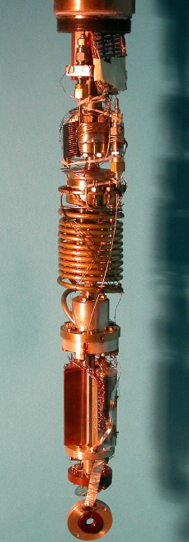
The nanostructures are characterized by measuring their electrical transport and noise properties as a function of temperature (10 mK to 300 K) and applied magnetic field (up to 17 T). Special measuring electronics (e.g. SQUID amplifier with a sensitivity of 10 pV/√Hz), low temperature measurement facilities as well as electromagnetically shielded rooms are available for high resolution measurements on nano-devices. Furthermore, the high-frequency properties of nanostructures can be measured up to 40 GHz.