Fabrication of nanostructered semiconductors by molecular beam epitaxy
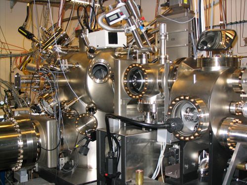
Molecular beam epitaxy (MBE) allows the control of semiconductor nanostructures with atomic precision. We concentrate in our group on GaAs- and Si-based materials systems and fabricate high quality heterostructures, quantum wells, and superlattices which are the basis for the realisation of lateral nanostructures like e.g. single electron transistors or quantum rings. Such devices allow for the control of single charges and spins. A special MBE technique, namely cleaved- and double cleaved edge overgrowth is used for the realisation of novel quantum wire and quantum dot devices which are test systems for future quantum information technology. We also study self-assembly and self-ordering of semiconductor quantum dots in lattice mismatched systems like Si/Ge and InAs/GaAs. Ordering of such quantum dots is achieved for example by combining cleaved edge overgrowth and self assembly where the cleavage plane provides an atomically precise template. Our high purity MBE machine in which also cleaved edge overgrowth is possible is shown in the figure.