Quantum transport in semiconductor nanostructures
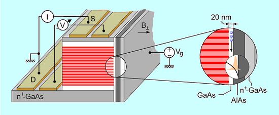
We fabricate semiconductor systems where electrons are quantum confined down to one or two dimensions, and investigate the unconventional conductance properties of the resulting novel condensates at low temperatures and high magnetic fields (e.g. Luttinger liquids, quantum Hall edges, striped quantum Hall phases, Mott transistors) The main fabrication method is molecular beam epitaxy (MBE) and especially overgrowth of cleavage planes in GaAs based heterosystems. This technique enables us to control single and coupled nanostructures with atomic precision and does not require any lithographic technique. The transport properties of such quantum wire systems are studied at mK temperatures and at high magnetic fields. An example of nano- and quantum transistors is a superlattice transistor as shown schematically in the figure. Other structures under investigation are two-dimensional systems bent by 90° and novel transistors fabricated from coupled chains of quantum dots. This project is supported financially by BMBF via nanoQUIT.
