Spintronic devices and sensors
The field of spin electronics has attracted broad interest over recent years due to a variety of both interesting physical phenomena and promising applications. The efficient use of the spin degree of freedom of charge carriers in "spintronic" devices requires materials with high spin polarization of the charge carriers at the Fermi level and high Curie temperature TC as well as the nano-engineering of these materials at interfaces and in device structures. Furthermore, the incorporation of the spin degree of freedom into nano-devices such as single electron transistors is of particular interest.
The research at the Walther-Meissner-Institute in the field of magnetic nanostructures for spintronics is directed in two main directions:
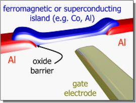
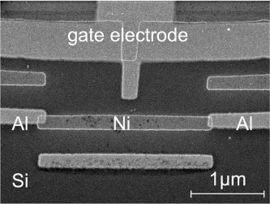
- The fabrication of single electron devices combining normal metal and superconducting elements with ferromagnetic parts. Here, the effect of the spin degree of freedom on the device functionality as well as the deliberate use of the spin degree of freedom to generate novel device functions is of particular interest.
- The fabrication of magnetic tunnel junctions based on half-metallic oxides allowing for a tunnelling magneto-resistance well above 100% at room temperature.