Simulations of transport in single molecules, thin organic films
The newly created Institute for Nanoelectronics deals on the one side with the development of modeling and design tools for semiconductor nanostructures and on the other with the fabrication and characterization of devices and components based on organic semiconductors
Molecular systems based on conductive polymers, carbon nanotubes, and other organic semiconducting materials are attracting more and more attention as building blocks for electronic, optoelectronic and sensor systems. This activity aims at the theoretical investigation of molecular devices and of the most suitable circuit architecture for their exploitation.
Main focus is towards the investigation of molecular optoelectronic and sensor systems based on a Cellular Nonlinear Network architecture, the design of Quantum Cellular Automata based on molecular nanostructures, and the simulation of molecular diodes and transistors.
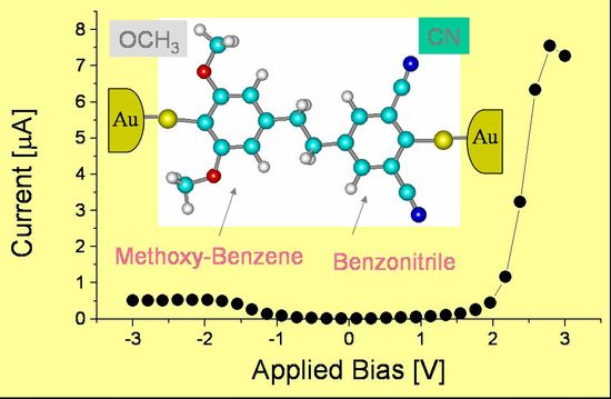
As an example, the figure shows how a single molecule between two metallic contacts displays the rectifying behaviour typical of semiconducting pn junctions. The result has been obtained by self consistently coupling a Green_function calculation of the current flowing through the molecule with a microscopic determination of the molecular orbitals.
Together with the design activity, an experimental effort is dedicated to the fabrication of organic electronic and optoelectronic devices, and to their electrical and electrooptical characterization. The main activities are the fabrication and characterization of Thin Film Transistor with organic active layers, and the fabrication and characterization of optoelectronic active devices (modulators, light emitters, photodiodes) based on conductive polymers and carbon nanotubes.
